Showing posts with label Advanced materials. Show all posts

Wednesday, 10 December 2014

Hacking into 3D Printers

Now a days, new 3D printers seem to be rolling out daily or at least the trends at the crowdsourcing sites indicate so. But how many of these campaigns will finally release a product in the market and will deliver to the mark at the claims made in these campaigns.
May be more than half, but with the expiry of lot important patents in the coming year this trend is going to go up on the rise with more new jargon and technologies being used in their crowdsourcing videos. The promise will be of 10x faster and 50x better technology.
Thus, we have decided to decipher these technologies for you and are going to post each week on a new 3D printing technology, with all what one needs to know to start a crowdsourcing campaign of his own or to decide whether to invest in the technology displayed in such campaigns.
Let us know the technology you want to be hacked in the comments

Tuesday, 9 December 2014

The Science behind HP's Fusion Jet 3D printer

HP has big claims and bigger hope for it's Fusion Jet 3D printer with which it entered the 3D printing space. HP or Hewlett Packard has made a fortune in the 2D printing business with its Inkjet and Laser printers, but never entered the 3D printing space, though the technology has been there since 1939. With the launch of its Fusion Jet 3D printer it made it clear that HP's technology in 2D space can be applied to the 3D realm as well.
The technology behind HP's fast and multi-color printing 3D fusion jet printer is based on a old IP that they hold for thermal inkjet printing and you can find the same technology being used in many of HP's 2D printers as well. They are a lot different from the Stereolithography or Material extrusion methods but quite similar to the laser sintering method without the laser.
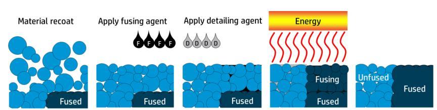
Laser sintering method spreads a layer of metal powder which is then sintered by precision lasers and then another layer of powder is spread onto it. The next layer when sintered is fused to the lower layer. This curing of material powder is attained in the fusion jet without the laser but a heat source and chemicals.
The Fusion jet spreads one layer of material and then a print head (thermal inkjet array) is passed onto it which prints chemicals across the entire print area. The print head has a dense no of nozzles per inch, with the total no. of nozzles on the entire print head being close to 30,000. This provides the highest resolution in 3D printing industry of 20 micron precision.
They use two types of chemicals - fusing agent and detailing agent with an option for a coloring agent. When they are heated by a energy source the fusing agent fuses the material while the detailing agent is used in areas where the effect of fusing agent has to be either removed or amplified. This allows to have nice surface finish with curves and sharp edges. This also allows to have a texture on the printed surface. The nozzles are capable of printing 3 million drops per second of such agents making it 10x more faster than any technology available so far. 

The major advantage of this technology is we can control the property of the printed mode with using different combination of agents and materials, also the ability of precisely print one voxel (volumetric pixel) with HP's proven technology in 2D printing allows you to print in such high defination that you are used to seeing in 2D prints from HP printers.
HP is right to making the claims it has for the printer but will need some time to polish the technology in 3D printing. But use of technology available in your normal 2D printer has allowed it to scale it both up and down and provide faster and better 3D printing at a affordable cost.
Have a look at what HP has to say about its Fusion Jet Printers (Yeah it does seem a bit far fetched but with the technology HP's using it is not that far away):

Saturday, 6 December 2014

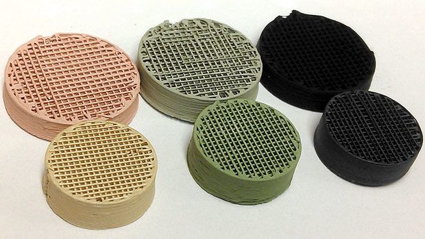
With this cartridge, you can print a Solid Oxide Fuel Cell

Photo: Shah lab at Northwestern University

The mixture of ceramic, binder and solvent that evaporates at different rate allows you now to 3D print a solid oxide fuel cell. This ink is developed by researchers at Northwestern University. Prof. Ramille Shah is the man behind the ink, which allows 3D printing of all individual components of a fuel cell - anode, cathode, electrolyte and interconnects.
This work was shown at the Material Research Society fall meeting at Boston this week by Adam Jakus, a Ph.D. at Shah's lab. The use of 3D printing has allowed them to print in new shapes and designs which the conventional methods don't allow. They have been able to generate really dense packed particle structure in the 3D printed models. Moreover, 3D printing allows them to use new designs which might increase the surface area and hence the transport of charge or increase the efficiency. This can be one of the breakthroughs in use solid oxide fuel cell to convert gas into electricity.

Also, the team has developed a ink to 3D print GRAPHENE!

3D Printing a Kidney - TED talk

See how 3D printing is revolutionising the medical world and could help us lead better and longer lives in this TED talk by Surgeon Anthony Atala:

4D printing is more real than you can think

3D printing is the current hype in the tech world. People are amazed with the ability to print their imagination in 3D and do all kind of stuff with it. Its a boon for artists and innovators. While the world is looking to expand the horizon of 3D printing, there is a group of people who are thinking about 4D printing.
4D printings adds the dimension of time to materials i.e. programmable materials which can self assemble or disassemble in real time depending on the type of stimuli. The idea of 4D printing comes from shape memory alloys which used thermoelastic displacive transformation like thermoelastic martensitic transformation to change shape with stimuli.
But advances in 4D printing is going to herald a new era of materials that can build themselves. The MIT's Self Assembly lab is working on the technology of 4D printing. They are currently printing interwoven materials with different thermal properties thus on exposing to temperature change they tend to behave similar to shape memory alloys.

Monday, 14 April 2014

Cool Hot Electronic Devices using Electropolymerization

Scientists at Georgia Institute of Technology,  have successfully increased the thermal conductivity of Polymers by 20 times. They have used Electropolymerization to produce aligned array of nano-fibers. The thermal interface material can operate at temperatures as high as 200 degrees Celsius.

The material has been fabricated on  heat sinks and heat spreaders and adheres well to devices, potentially avoiding reliability challenges that are caused by differential expansion in other conducting materials. The new material can be used to conduct heat away from LEDs, servers, automobiles and certain mobile devices.

“Thermal management schemes can get more complicated as devices get smaller,” said Baratunde Cola, an assistant professor in the George W. Woodruff School of Mechanical Engineering at the Georgia Institute of Technology. “A material like this, which could also offer higher reliability, could be attractive for addressing thermal management issues. This material could ultimately allow us to design electronic systems in different ways.”
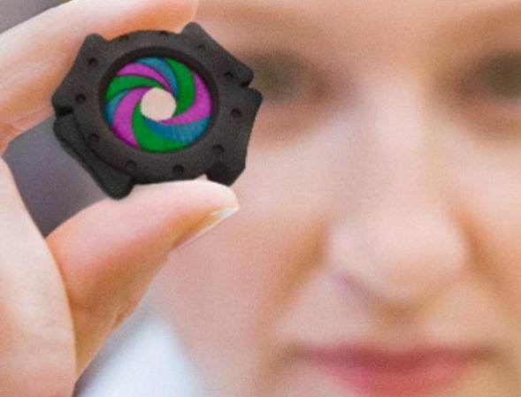
Testing Polymer Thermal InterfaceResearch scientist Virendra Singh, from the George W. Woodruff School of Mechanical Engineering at Georgia Tech, holds a test sample used to measure thermal conductance and thermal cycle reliability in a new polymer material developed to remove heat from electronic devices. (Georgia Tech Photo: Candler Hobbs)

The research, which was supported by the National Science Foundation, was reported March 30 in the advance online publication of the journal Nature Nanotechnology. The project involved researchers from the Georgia Institute of Technology, University of Texas at Austin, and the Raytheon Company. Virendra Singh, a research scientist in the Woodruff School, and Thomas Bougher, a Ph.D. student in the Woodruff School, are the paper’s co-first authors.

Amorphous polymer materials are poor thermal conductors because their disordered state limits the transfer of heat-conducting phonons. That transfer can be improved by creating aligned crystalline structures in the polymers, but those structures – formed through a fiber drawing processes – can leave the material brittle and easily fractured as devices expand and contract during heating and cooling cycles.
The new interface material is produced from a conjugated polymer, polythiophene, in which aligned polymer chains in nanofibers facilitate the transfer of phonons – but without the brittleness associated with crystalline structures, Cola explained. Formation of the nanofibers produces an amorphous material with thermal conductivity of up to 4.4 watts per meter Kelvin at room temperature.
The material has been tested up to 200 degrees Celsius, a temperature that could make it useful for applications in vehicles. Solder materials have been used for thermal interfaces between chips and heat sinks, but may not be reliable when operated close to their reflow temperatures.
“Polymers aren’t typically thought of for these applications because they normally degrade at such a low temperature,” Cola explained. “But these conjugated polymers are already used in solar cells and electronic devices, and can also work as thermal materials. We are taking advantage of the fact that they have a higher thermal stability because the bonding is stronger than in typical polymers.”
The structures are grown in a multi-step process that begins with an alumina template containing tiny pores covered by an electrolyte containing monomer precursors. When an electrical potential is applied to the template, electrodes at the base of each pore attract the monomers and begin forming hollow nanofibers. The amount of current applied and the growth time control the length of the fibers and the thickness of their walls, while the pore size controls the diameter. Fiber diameters range from 18 to 300 nanometers, depending on the pore template.
After formation of the monomer chains, the nanofibers are cross-linked with an electropolymerization process, and the template removed. The resulting structure can be attached to electronic devices through the application of a liquid such as water or a solvent, which spreads the fibers and creates adhesion through capillary action and van der Waals forces.
“With the electrochemical polymerization processing approach that we took, we were able to align the chains of the polymer, and the template appears to prevent the chains from folding into crystals so the material remained amorphous,” Cola explained. “Even though our material is amorphous from a crystalline standpoint, the polymer chains are highly aligned – about 40 percent in some of our samples.”
Though the technique still requires further development and is not fully understood theoretically, Cola believes it could be scaled up for manufacturing and commercialization. The new material could allow reliable thermal interfaces as thin as three microns – compared to as much as 50 to 75 microns with conventional materials.
“There are some challenges with our solution, but the process is inherently scalable in a fashion similar to electroplating,” he said. “This material is well known for its other applications, but ours is a different use.”
Engineers have been searching for an improved thermal interface material that could help remove heat from electronic devices. The problem of removing heat has worsened as devices have gotten both smaller and more powerful.
Rather than pursue materials because of their high thermal conductivity, Cola and his collaborators investigated materials that could provide higher levels of contact in the interface. That’s because in some of the best thermal interface materials, less than one percent of the material was actually making contact.
“I stopped thinking so much about the thermal conductivity of the materials and started thinking about what kinds of materials make really good contact in an interface,” Cola said. He decided to pursue polythiophene materials after reading a paper describing a “gecko foot” application in which the material provided an estimated 80 percent contact.
Samples of the material have been tested to 200 degrees Celsius through 80 thermal cycles without any detectable difference in performance. While further work will be necessary to understand the mechanism, Cola believes the robustness results from adhesion of the polymer rather than a bonding.
“We can have contact without a permanent bond being formed,” he said. “It’s not permanent, so it has a built-in stress accommodation. It slides along and lets the stress from thermal cycling relax out.”
In addition to those already mentioned, co-authors of the paper included Professor Kenneth Sandhage, Research Scientist Ye Cai, Assistant Professor Asegun Henry and graduate assistant Wei Lv of Georgia Tech; Prof. Li Shi, Annie Weathers, Kedong Bi, Micheal T. Pettes and Sally McMenamin in the Department of Mechanical Engineering at the University of Texas at Austin; and Daniel P. Resler, Todd Gattuso and David Altman of the Raytheon Company.
A patent application has been filed on the material. Cola has formed a startup company, Carbice Nanotechnologies, to commercialize thermal interface technologies. It is a member of Georgia Tech’s VentureLab program.
This research was supported by the National Science Foundation (NSF) through award CBET-113071, a seed grant from the Georgia Tech Center for Organic Photonics and Electronics and an NSF-IGERT graduate fellowship. Any conclusions or opinions are those of the authors and do not necessarily represent the official views of the NSF.
CITATION: Virendra Singh, et al., “High thermal conductivity of chain-oriented amorphous polythiophene,” (Nature Nanotechnology, 2014). http://www.dx.doi.org/10.1038/nnano.2014.44